
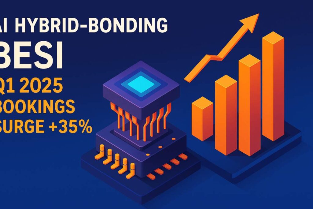
In a world racing to train ever-larger AI models, the interconnects between chip layers have become the new battleground. Enter AI hybrid-bonding—a technology that fuses dies copper-to-copper, unlocking ultra-high bandwidth and razor-thin form factors. In Q1 2025, BE Semiconductor Industries (Besi) shattered expectations with a 35% sequential rise in order bookings, demonstrating that hybrid-bonding is no longer a niche play but a core driver of the semiconductor revolution.
What Is Hybrid-Bonding and Why It’s Critical for AI
Traditional chip stacking uses micro-bumps—tiny solder balls—to link dies. As AI workloads balloon, those bumps create bottlenecks:
- Bandwidth constraints as data shuttles across resistive paths.
- Power inefficiencies from longer interconnects.
- Size limits that hamper compact, multi-die modules.
By contrast, hybrid-bonding replaces bumps with direct copper bonds at nanometer precision:
- Massive bandwidth gains, vital for inference and training of trillion-parameter models.
- Lower power thanks to reduced electrical resistance.
- Slimmer stacks, enabling dense 2.5D/3D-IC solutions for both data centers and edge devices.
Industry analysts forecast the advanced-packaging market doubling from $14 billion in 2024 to $28 billion by 2028, with hybrid-bonding leading growth .
AI Demand Thriving: Driving the Hybrid-Bonding Boom
Three converging trends are turbocharging hybrid-bonding:
- Hyperscale GPU Clusters
Tech giants racing to deploy next-gen GPUs need High-Bandwidth Memory (HBM 4) stacks—only reliably produced via copper bond tools. - Edge-AI Proliferation
From autonomous drones to AR glasses, compact AI inferencing devices demand small, power-efficient modules. - Logic-Node Shrinkage
Foundries at 3 nm and below require sub-100 nm alignment tolerances to preserve wafer yields—hybrid-bonding delivers.
These forces have shifted Besi’s order book: AI-related bookings now account for over 60% of total Q1 2025 orders .
Besi’s Q1 2025 Performance in Detail
| Booking Segment | Q4 2024 (€ M) | Q1 2025 (€ M) | % Change QoQ |
|---|---|---|---|
| Hybrid-Bonding Tools | 71.1 | 114.2 | +61% |
| Other Advanced Tools | 47.4 | 45.8 | –3% |
| Total Orders | 118.5 | 160.0 | +35% |
Besi’s Q1 bookings jumped from €118.5 M to €160 M—an 8-quarter high and a clear sign that AI packaging is the company’s fastest-growing segment .
The Three Pillars Behind the 35% Surge
1. Data-Center AI Deployments
Two leading memory manufacturers placed multi-million-euro orders for HBM 4 hybrid-bonding tools, directly tying Besi’s tools to the backbone of large-scale LLM training.
2. Strategic Foundry Partnerships
A top Asian foundry—pushing logic processes to 3 nm and beyond—secured follow-on orders for Besi’s sub-100 nm alignment platforms, a testament to their precision and yield impact.
3. First-Mover Advantage
With over 70 installations worldwide, Besi’s machines deliver the fastest cycle times and lowest defect rates. That track record keeps legacy bump-based toolmakers playing catch-up.
Insights from Industry Experts
“Hybrid-bonding has gone from lab curiosity to production linchpin,” says Dr. Anita Verma, Senior Packaging Engineer at a leading GPU firm. “It’s the only way to scale bandwidth without exploding power budgets.”
Richard Ma, Analyst at TechInsights, adds:
“Besi’s Q1 bookings are a bellwether for AI cap-ex. We see sustained double-digit growth through 2026 as HBM 5 and co-packaged optics enter development.”
Broader Implications for the Semiconductor Ecosystem
- Chip Architects gain freedom to design 3D-ICs without bump constraints.
- Tool Vendors must innovate complementary solutions—look for fan-out wafer-level packaging (FOWLP) to rise.
- Investors can use Besi’s order momentum as a proxy for AI infrastructure spending.
Future Outlook: Q2 2025 and Beyond
Besi forecasts flat to +5% revenue growth in Q2 2025 amid trade-war headwinds. Yet three catalysts loom:
- HBM 5 Rollouts (Late 2025): Anticipated to trigger a fresh wave of tool orders.
- Co-Packaged Optics: Hybrid-bonded dies integrated with photonics for sub-nanosecond interconnects.
- Edge-AI Miniaturization: Demand for compact, high-bandwidth modules in drones, robotics, and wearables.
These trends suggest hybrid-bonding’s runway extends well beyond the data center, embedding itself in every AI-enabled device.
Conclusion
Besi’s 35% bookings surge in Q1 2025 isn’t just a quarterly win—it validates AI hybrid-bonding as the defining packaging technology for the next AI era. From hyperscale data centers to handheld edge devices, copper-to-copper bonds are rewriting the rules of performance, power, and size. Stakeholders across the semiconductor chain must adapt, innovate, and invest in hybrid-bonding to stay ahead.
Call to Action
What AI packaging trends excite you most? Share your thoughts on hybrid-bonding’s future in the comments below—and subscribe to TransformInfoAI for weekly deep dives into the technologies shaping tomorrow.


